J. Donald Tillman
20 July 2003
This is a basic implemention of the Quadrature Trapezoid Voltage
Controlled Oscillator (VCO). It serves as a practical
example of the theory and concepts described in the first article in
series.
This oscillator presented here is just the VCO core, and it is
likely that other more practical waveforms will be derived from
it. That circuitry will be covered in future articles.
Functional Description
There are two sets of inputs, one for exponential control and one
for linear control. Exponential control can tune the frequency
over a very wide range, enables tuning musical intervals, and can
effectively set the range of the linear control. Linear
control, besides providing a useful linear control function, can be
used for FM Synthesis, and is centered about 0 Hz so it can swing
between positive and negative frequencies. The linear control
is effectively muliplied by the exponential control.
The exponential control section consists of two control voltage
inputs and a "Tuning" pot. These are summed together and have
the standard sensitivity of 1.0 V/octave, so an increase of 1.0 V
will double the frequency.
The linear control section consists of two control voltage inputs
and a "Frequency" pot. These are scaled linear inputs;
they are summed and the resulting value is multiplied by the
exponential control. Thus if +1.0 V would be the reference
value, +2.0 V would be twice that frequency, 0.0 V would be zero Hz,
and -1.0 V would be the negative frequency.
The intended range of each control voltage input is from -10.0 V to
+10.0 V. The net range of control (summing the two control
voltages and the potentiometer value for a given control set) is
between -5.0 and +5.0 V, with some additional headroom.
For simpliciy I have left input potentiometers off of the
schematic. Feel free to add them or modify the input sections
to taste. Fine tuning pots would be a reasonable addition,
for instance.
This circuit has four quadrature waveform outputs
(+TSin, +TCos, -TSin and -TCos).
The output waveforms range from -5.0 V to +5.0 V. Additionally
there are two state outputs, StateA and StateB, for
waveshaping, free square waves, and other uses.
Schematic
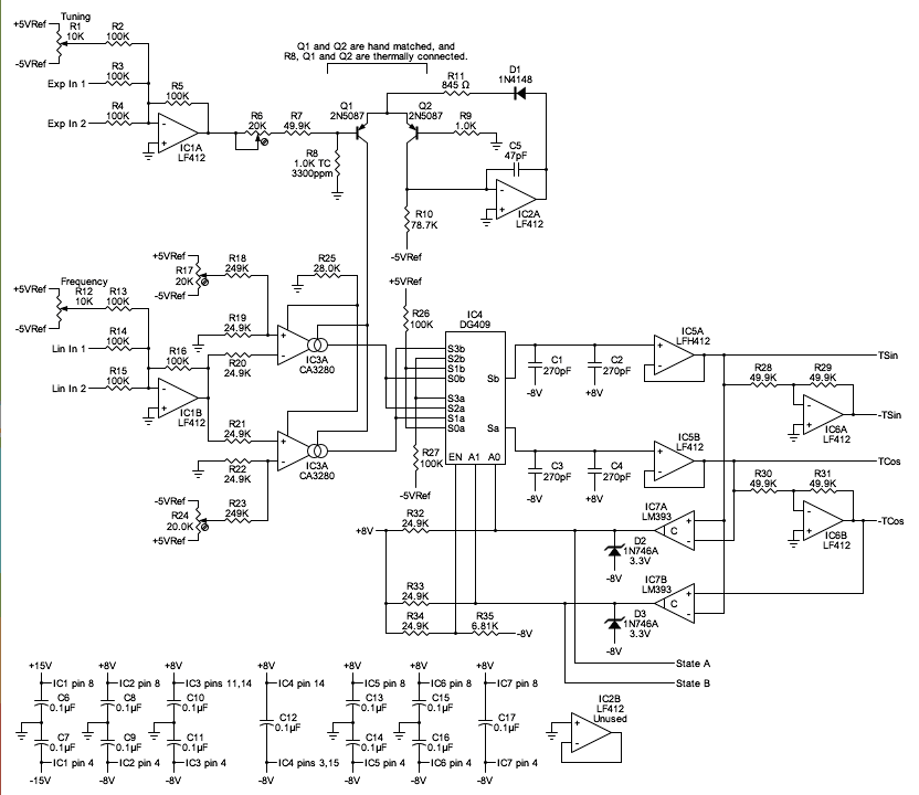
Here is the schematic of the Quadrature Trapeoid VCO:
Circuit notes:
C1 through C4 are 270 pF poly caps, hand matched. Or 0.068
uF for a Low Frequency Oscillator (LFO). (See below.)
C5 is a 47 pF ceramic or mica cap.
C6 through C17 are 0.1 uF ceramic caps.
IC1,IC2,IC5 and IC6 are LF412 dual opamps.
IC3 is a CA3280 dual OTA.
IC4 is a DG409 dual 4-input analog multiplexer.
IC7 is an LM393 dual comparator.
R1 and R12 are 10K panel mount potentiometers, the "Tuning" and
"Frequency" controls respectively.
R8 is a 1.00K ohm 3300ppm tempco resistor.
R17 and R24 are 20K ohm trimpots.
All other resistors are 1/4 watt, 1% units.
Q1 and Q2 are 2N5087 PNP transistors, hand matched in the circuit
shown later in this article.
R8, Q1 and Q1 are thermally connected together.
Note: I try to use the primary manufacturer's pin designations
throughout the schematic. However, the 1-based pin
designations on the Siliconix DG409 data sheet are ridiculous, so
I made up my own designations for all of the pins.
Design Notes
First the IC choices:
LF412's were choosen for the opamps throughout this circuit for
their low offset voltage, near zero input bias current, high
speed, and being unity gain stable.
The CA3280 dual Operational Transconductance Amp (OTA's) was
chosen for its low noise, it's linearization circuitry, and that
it comes in matched pairs.
The Siliconix DG409 was selected over the standard CMOS CD4052
multiplexer because of the DG409's low charge injection, and this
is exactly the type of application where charge injection will
have a bad effect.
An LM393 was chosen for the comparator becuase of its high speed
and low power dissipation.
Opamp IC1A sums the exponential control voltage inputs and
inverts. R6, R7 and R8 divide down the 1.0 V/oct control
voltage to 18 mV/oct. R8 is a tempco resistor with a 3300 ppm
temperature sensitivity, but you can use a standard resistor if you
care less about accurate tuning. R6 trims the scale to
1.0V/oct.
Q1, Q2, IC2A, R9 through R11, and C3 implement a classic exponential
converter topology. There are a couple of subtle differences
between this one and, say, the exponential converter in the ASM-1 or
in National Semiconductor's application note AN-30. This uses
discrete, hand matched PNP transistors instead of an integrated NPN
transistor array. I do this because a positive current source
is needed for the OTA's, because it's much easier to hand match
transistors than to deal with PNP transistor array availability, and
because discrete transistors can have significantly better
performance than most integrated PNP transistors, especially with
the important beta and RBE parameters. Another
departure from the typical exponential converter implementation is
that the input is applied to the current output transistor instead
of to the offset transistor, and so the opamp just holds the emitter
voltage constant and isn't in the signal path. (The opamp will
follow the exponential signal due to the voltage drop across R11,
but that's a secondary effect.)
R11 sets the maximum limit of the output current of the exponential
converter. Here that's 8.0 mA (4.0 mA per OTA). The OTAs
are rated for an Iabc of up to 10.0 mA each, so this is
safely below that value.
R10 and the -5.0 V reference voltage set the center bias current,
the current the exponential converter delivers with a 0.0 V
exponentional control input.
The value of the exponential converter's center bias point is
determined by deciding upon a maximum running power dissipation for
the OTA's and working backwards. (I'll use the
phrase maximum running to mean the maximum value over the
spec'd range. One can still take it over the spec'd range with
reduced accuracy before the hard limiting kicks in.)
Select 1/8 watt as the maximum running dissipation for the CA3280
dual OTA chip. The chip isn't especially temperature
dependent the way it is being used here, but in the interest of
accuracy we need to minimize heating effects.
The OTA's run off of the ± 8.0 V power supply, so 1/8 Watt
means a roughly 4 mA supply current per OTA. This is an
advantage of running the chip at a reduced supply voltage; at a
full ±15V power supply the heating effect would roughly
double.
The CA3280 data sheet tells us that the OTA supply current is
about 4 times the amplifier bias current, Iabc.
So the maximum running Iabc should be about 1mA.
Since the exponential converter drives both halves of the CA3280
dual OTA, it should have a maximum running output current of
2mA. (I'm going to tweak that up to 2.048 mA to make a table
prettier later on.) That's the value with the exponential
control voltage sum at +5.0V (spec'd above).
And with an exponential input control voltage of 0.0 V, the
exponential converter should be 1/25 times the maximum
running value. Or 64.0 μA. And this determines R10.
On the linear control side, IC1B generates the inverted sum of the
scaled linear control voltage inputs and this is presented to the
IC3A and IC3B, a pair of OTA's in a push-pull arrangement.
IC3A and IC3B are a pair of OTA's in a push-pull arrangement.
We take advantage of the CA3280's input linearization diodes which
attenuate the input signal and correct for the nonlinearites in the
differential amplifier transfer curve. This is described well
in the CA3280 data sheet. Here the values of R19-R22 and R25
are chosen for an input swing of ±6.0 V providing a little
headroom over the ± 5.0 V spec'd input range. R25
sets the diode current to 120 μA per OTA.
C1 through C4 are the ramping capacitors. The capacitors are
split between the ±8V power supply instead of being connected
to ground to avoid sudden current changes in the ground line.
IC4 is a DG409 analog multiplexer that steers the four input sources
to the ramping capacitors. Those four input sources are the
control current off of IC3A, the inverted control current off of
IC3B, the postive reference voltage, and the negative reference
voltage.
A pair of voltage follower opamps, IC5A and IC5B, buffer the
capacitor signals and a pair of inverting opamps, IC6A and IC6B,
provide inverted signals.
Comparators IC7A and IC7B switch states when the ramping output
overcomes the held output. The LM393 outputs are open
collector so they need pull-up resistors R32 and R33.
Zener diodes D2 and D3 limit the voltage swing of the comparator
outputs to about 3.3 V above the -8.0 V power supply. The
DG409 data sheet specifies the maximum low and minimum high digital
input voltages at 0.8 V and 2.4 V respectively, and with the
comparator output signal limited to 3.3 V it covers those limits
symmetrically.
There's nothing mentioned about this in the data sheet, but I found
out the hard way that the DG409 behaves badly when large voltage
swings (16.0 V in this case) are applied to the digital
inputs. Specifically the multiplexer deposits a substantial
negative charge on one of the capacitors during certain
transistions. So that's why the zeners are there. As a
nice side effect the zeners minimize the size of voltage transients
in the circuit as well as minimizing current transients that might
affect the power supply.
Power Supply Issues
The entire circuit is designed to operate off an MOTM-style power
source, using Don's modular synthesizer power supply rules.
I'll formalize those at some point in a later article, but for now
the rules can be stated as:
- ±15.0 V is supplied to all the modules from an
off-the-shelf linear supply.
- A module's operation should not depend on the supply voltage
to be especially accurate or clean.
- If the circuit needs a precise voltage, that voltages should
be created locally to the module.
- The circuit should take care not to disturb the power supply
with current transients.
- The circuit should take extra care not to disturb the analog
ground with current transients or dc current draw. If
there is a need to pass significant current to ground, there
should be a separate "dirty" ground available.
The overall effect is that the modules should not depend on the
power supply being perfect, but that things will be all that much
better if it is, and each module does what it can to be a nice
neighbor.
The "+15 V" and "-15 V" points in the schematic are the main
±15.0 V power supply lines.
The "+8 V" and "-8 V" points in the schematic are from a small
on-board ±8.0 V local power supply.
The "+5VRef" and "-5VRef" points in the schematic are locally
generated ±5.0 V reference voltages and cannot supply
significant amounts ofcurrent. They are used for tuning the
VCO, for the exponential converter and for setting the amplitude of
the waveform.
Almost all of the VCO circuitry runs off of the local ±8.0 V
supply. There are a number of reasons for that:
- it reduces the power dissipation of the CA3280 dual OTA,
reducing the heating and accompanying thermal drift,
- provides more accurate tuning by keeping the Vee line of the
CA3280 dual OTA independant of the -15.0 V supply
- allows a smaller emitter resistor in the exponential
converter, minimizing the voltage swing at the output of
IC2A
- allows fewer transients from this circuit off the ±15.0 V
power supply lines
- insulates much of the circuit from any the ±15.0 V
supply
Here is the schematic of the power supply and voltage references:
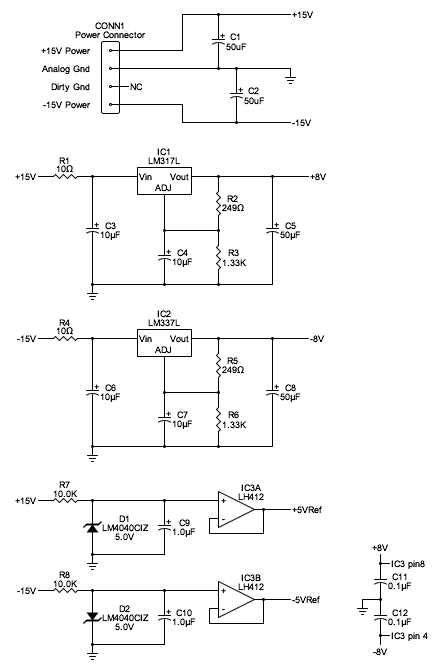
Schematic of the power supply and voltage references.
|
Power supply notes:
The power supply connector is an MTA-156 type (following the
SynthTech MOTM).
IC1 and IC2 are LM317L and LM337L TO-92 packaged voltage
regulator chips.
D1 and D2 are LM4040CIZ-5.0V voltage references.
C1 through C10 are electrolytic capacitors.
C11 and C12 are ceramic capacitors.
All resistors are 1/4 Watt 1% units.
Tuning
I'm going to use the term Reference Frequency to describe the
VCO running frequency resulting from a 0.0 V exponential control and
a 1.0 V scaled linear control. This is a somewhat arbitrary
definition and various other applications of this circuit might
consider a different choice.
The linear control voltage is first attenuated by the OTA input
linearization diodes. That attenuation is:
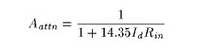
Where
Aattn is the attenuation of the linearizing
diodes expressed as a gain.
Id is the linearizing diode current in amperes.
Rin is the total input resistance to the OTA in
ohms (the sum of the two input resistors).
(This equation comes from the CA3280 data sheet, incorporating the
input resistors and tweaking the units to something more consistent.)
A linearizing diode current of 120 μA and an input resistance
of 49.8K (R19 + R20, or R21 + R22) result in an attenuation factor,
Aattn, of 0.0115.
The output current of the either of the OTAs is:
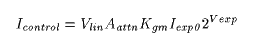
Where:
Icontrol is the ramping current to the
capacitors, in amperes.
Vlin is the linear input control voltage, in
volts.
Aattn is the attenuation factor, expressed as a
gain, calculated above.
Kgm is the transconductance gain factor, the
ratio of the OTA transconductance to bias current. For a
CA3280 that value is 16.0 V-1 according to the data sheet.
Iexp0 is the value of the OTA bias current, in
amperes, when the exponential input control voltage is zero.
Vexp is the exponential input control voltage,
in volts.
At the reference frequency, Icontrol is thus 5.89 μA.
The frequency of the VCO is:

Where:
Fvco is the frequency the VCO runs at, in
hertz.
Icontrol is the ramping current to the
capacitors, in amperes, calculated above.
Vpp is the peak-to-peak voltage swing of the
trapezoid waveform.
C is the value of the timing capacitors. In this
circuit would be the parallel combination of C1 and C2, or
the parallel combination of C3 and C4.
For an audio VCO one might choose middle C, 261.6 Hz, as the
reference frequency. This works out to a capacitance value of
563 pF. Split between two capacitors of standard value, that's
270 pF for each of C1 through C4.
The tuning range then looks like this:
| Control Voltage |
OTA Bias Currrent |
Frequency |
Notes |
| +5.0 V | 1.024 mA | 8372 Hz |
| +4.0 V | 512 μA | 4186 Hz | Top piano note |
| +3.0 V | 256 μA | 2093 Hz |
| +2.0 V | 128 μA | 1046.5 Hz |
| +1.0 V | 64 μA | 523.3 Hz |
| 0.0 V | 32 μA | 261.6 Hz | Middle
C |
| -1.0 V | 16 μA | 130.8 Hz |
| -2.0 V | 8 μA | 65.4 Hz |
| -3.0 V | 4 μA | 32.7 Hz | Organ pedal
C |
| -4.0 V | 2 μA | 16.35 Hz |
| -5.0 V | 1 μA | 8.176 Hz |
|
LFO Tuning
The VCO can also be tuned to low frequencies with only a change in
capacitor value. For a reference frequency of 1.0 Hz, that
works out to a C of 0.147 μF split between two capacitors of
standard value, or 0.068 μF each for C1 through C4.
The resulting tuning range looks like this:
| Control Voltage |
OTA Bias Currrent |
Frequency |
Notes |
| +5.0 V | 1.024 mA | 32.0 Hz |
| +4.0 V | 512 μA | 16.0 Hz | |
| +3.0 V | 256 μA | 8.0 Hz |
| +2.0 V | 128 μA | 4.0 Hz |
| +1.0 V | 64 μA | 2.0 Hz |
| 0.0 V | 32 μA | 1.0 Hz | Reference frequency |
| -1.0 V | 16 μA | 0.5 Hz |
| -2.0 V | 8 μA | 0.25 Hz |
| -3.0 V | 4 μA | 0.125 Hz | |
| -4.0 V | 2 μA | 0.0625 Hz |
| -5.0 V | 1 μA | 0.0313 Hz |
|
Construction Suggestions
Use of the best electronic construction practices will pay off in
the performance of this circuit. Especially grounding issues.
Transistors Q1 and Q2 should be hand matched. And transistors
Q1 and Q2 should be mounted in a tight thermal connection to R8.
You should hand match the value of C1 || C2 with the value of C3 ||
C4.
Power supply decoupling capacitors should be mounted close to their
respective ICs.
Transistor Matching
Transistor Q1 and Q2 should be closely matched, and mounted with a
good thermal connection between them and to resistor R8.
I'm a big fan of not just generically matching transistors, but to
match the specific parameters that the circuit requires, under
conditions very similiar to the actual circuit. For this VCO I
would recommend matching the base to emitter voltage, VBE
with a zero collector to base voltage and a collector current of 32
μA.
I recommend this circuit:
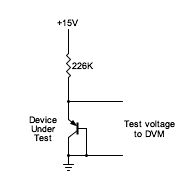
Transistor matching circuit.
|
(Note: This circuit draws very little current and some power
supplies have a minimum current draw requirement to work
at spec. You may need to add a resistor of around 1.5 K
across the power supply terminals.)
I would recommend getting a batch of 25 or so transistors, they are
very inexpensive, and using a good quality digital multimeter to
find two that are closest in value. This shouldn't be
difficult; out of batch of 25 I recently tested, all were within 5
mV.
Assure that the work area is free from any temperature changes such
as breezes. If you handle the transistors with pliers your
fingers won't heat them up. The usual precautions.
Calibration
Trimpot R6 should be adjusted for an exact 1.0 V / Octave
sensitivity at the exponential inputs.
Trimpots R17 and R24 are used to null out the offset voltages of
the OTA's. A common offset for the two OTAs will have an
effect of moving the 0.0 Hz point of the linear frequency control
inputs. An offset difference between the two OTAs will have
an effect of jittery performance near 0.0 Hz.
A good way to adjust R17 and R24 is to
-
Ground the exponential and linear control voltage inputs.
Set R1, the Tuning pot, a little below halfway. Set the
Frequency pot, R12, to center and ground the wiper of R12.
-
Short R35, disabling IC4, the analog mulitplexer.
-
Monitor the output of IC3A with a digital multimeter and adjust
trimpot R17 for a zero crossing.
-
Monitor the output of IC3B with a digital multimeter and adjust
trimpot R24 for a zero crossing.
If you need to measure the output currents of the OTAs for any
testing or calibration work, it's easiest to disconnect them from
the capicitors and the rest of the circuit by shorting R35,
disabling the multiplexer chip.
References
CA3280 Dual Operational Transconductance Amplifier,
Intersil data sheet.
DG408/DG409 8-Channel/Dual 4-Channel High Performance CMOS Analog
Multiplexers,
Siliconix data sheet.
LF412 Low Offset, Low drift Dual JFET Input Operational
Amplifier,
National Semiconductor data sheet.
LM193/LM293/LM393 Low Power Low Offset Voltage Dual
Comparators,
National Semiconductor data sheet.
LM4040 Precision Micropower Shunt Voltage Reference,
National Semiconductor data sheet.
Log Converters Application Note AN-30,
National Semiconductor.
ASM-1 Analog Synthesizer Module,
Gene Stopp and Magnus Danielson.
Updates
19 July 2003 Originally published.
20 July 2003 Add this updates section, fix LF412 designations
in schematic.
24 July 2003 Fix IC designations in power supply schematic,
fix various typos and language goofs.
29 February 2004 Nicer HTML layout, fixed an error in the
calibration procedure.