J. Donald Tillman
January 1999
Abstract
This is an original design for an interpolating scanner, a circuit
with a number of signal inputs, a control voltage input and a signal
output. The output effectively selects between the inputs, fading
from one to the next, as the control voltage rises.
Prior scanner circuits include:
-
the electromechanical scanner used on Hammond Organs (ref) which uses
capacitive coupling between spinning metal plates.
-
Juergen Haible's interpolating scanner
which uses opamp circuits generating triangular windows
to drive current controlled amplifiers.
-
A two-channel panner circuit might be considered a degenerate form of
a scanner. The data sheet for the Precision Monolithics, Inc.
SSM-2024 current-controlled amp IC shows a
stereo panner, they call it an "Exponential Cross-Fade Controller",
where two CCAs are controlled from a PNP differentialamp. The circuit
is pretty straightforward and I'm sure similiar circuits have been
used before.
The circuit presented here is inspired by and similiar to JH's scanner
except that drive circuit is an unusual extrapolation of the
differential amplifier topology used in the PMI panner. This approach
has some advantages:
-
a smoother transition between inputs
-
the total drive current (the sum of all the drive currents) is from a
constant current source assuring that the sum of the individual gains
is held constant
-
low parts count
-
control of the transition shape
The main disadvantage is that it requires transistor and diode
matching for best performance (although it seems to work pretty well
for unmatched devices).
The design is extendible to greater or fewer inputs.
Interface Requirements
For this particular design I'm using the following interface specs:
8 signal inputs.
Signal inputs are -10 dBu, 0.7 volts p-p, 50K ohms, DC to high audio
(roughly 20KHz).
Signal output is -10 dBu, 0.7 volts p-p, low impedance, DC to high
audio.
Control voltage input is between -2.5 and +2.5 volts, 50K ohms, DC
to high audio.
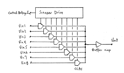
Scanner Design
Figure 1 below shows a block diagram of the Interpolating Scanner.
There is a Current Controlled Amplifer (CCA) of traditional design for
each signal input. Each CCA interfaces appropriately to the input
signal, has a current source output, and a gain (transconductance)
that is directly proportional to its control current input. The CCA
outputs are summed by shorting them directly together. A buffer
amplifier stage provides the appropriate output level and impedance.
|
|
Figure 1. Block diagram of the interpolating scanner.
|
The CCAs are transconductance amplifiers; the input is a voltage, the
output is a current, the gain is linearly proportional to the control
current, and in this case the control current is expected to be from
0.0 to 2.0 mA. More on this later.
Figure 2 below shows the details of the Scanner Drive circuit.
Figure 3 below shows schematics of the CCAs and the buffer amp.
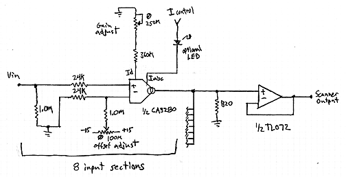
Figure 3. Current Controlled Amplifier and Buffer Amp.
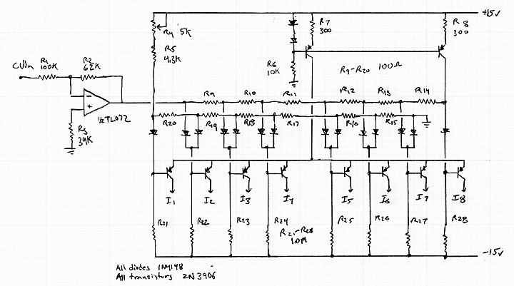
Scanner Drive Theory of Operation
In the schematic above, the opamp provides a flexible interface to
the outside world (you can add multiple inputs here as well as manual
controls), scales the control voltage slightly, and supplies a low
impedance source of the control voltage to the rest of the circuit.
The issue in extending a diff amp to more than two inputs is to not
only gradually turn one transistor off and another on, but also turn
that second one off and the next one on in the same manner.
Resistors R9 through R14 provide 190mV voltage steps up from the
control voltage and resistors R15 through R20 provide 190mV voltages
steps up from ground. The diodes select the higher of the two values.
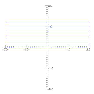 Here are three plots I drew to show how this works.
The X axis is the voltage tapped off of the opamp in volts and the Y
axis is the various base voltages in volts. For clarity, the base
voltages here are before the base diodes so offset everything
down by one diode voltage drop to get the actual base voltages.
In the first plot we see the constant voltages presented by the
resistor string on the right. These are 190 mV apart.
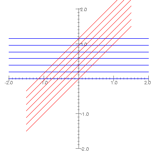 In the second plot we also see a string of input signal voltages,
presented by the resistor string on the left. These voltages are also
190mV apart.
In the second plot we also see a string of input signal voltages,
presented by the resistor string on the left. These voltages are also
190mV apart.
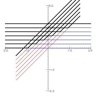 In the third plot we see the effect of the diodes, selecting the most
positive of each of the voltage pairs. Again, for clarity this diagram
shows voltages before the diode voltage drop. Note that the extreme
outputs are not paired. Also note that the voltage between crossover
points is two voltage steps.
In the third plot we see the effect of the diodes, selecting the most
positive of each of the voltage pairs. Again, for clarity this diagram
shows voltages before the diode voltage drop. Note that the extreme
outputs are not paired. Also note that the voltage between crossover
points is two voltage steps.
Shape Control
There is some control over the shape of the interpolation curve. The
circuit presented above is optimized for a smooth and complete
transition from one stage to the next, but by varying the control
voltage swing and the difference between the voltage steps you can
customize the curves.
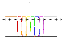
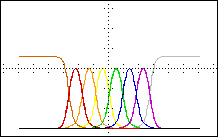
Here are three plots from a SPICE simulation of the scanner drive
circuit. All have the input control voltage on the X axis, 1 volt per
division, and the individual output currents on the Y axis, 0.5mA per
division, with EIA colors representing output currents I1 through I8.
The first plot is with double the step voltage and shows very sharp
transistions. It is the scanner drive circuit above with the
following values changed:
step voltage = 380mV
R2 = 33 k
R4,5 = 3.3k
R8 = 150
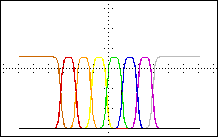
The second plot is the schematic above.
step voltage = 190mV
R4,5 = 6.8k
The third plot is with roughly half the step voltage. Note that at the
extremes of the input range all of current from the current source is
channeled through I1 or I8, but the intermediate outputs have so much
spread that they steal from their neighbor's peak currents as the sum
current stays constant.
step voltage = 90mV
R2 = 33k
R4,5 = 16k
R8 = 620
A potential strategy for an optimal shape would be to select step
voltage value where the I2 through I7 peak currents are 95% of the I1
or I8 shelf currents; 95% percent being a somewhat arbitrarily choosen
value near unity. It is possible to calculate an approximation to the
appropriate step voltage by solving the equation of a differential amp
in this situation:
Vstep = 2 * 0.026 * ln( 2 * (Rp / (1-Rp)))
Where Vstep is the step voltage and R is
the ratio of the peak current of one of the intermediate outputs (I2
through I7) to the shelf current of the outside stages (I1, I8). For
Rp = 0.95, Vstep is 190 mV, and this is the value used in the
schematic.
Matching Issues
Do the transistors in this circuit need to be matched? Close matching
is not required, and depending upon the application, none may be
necessary. For most electronic music applications I would suggest the
minimal matching procedure: check the forward voltage of the diodes
and the emitter-base junctions of the transistors at some low current,
say 100 uA, and throw out the ones with extreme numbers.
I built a breadboard version of this circuit without matching the
transistors, and differences in the curves of the individual outputs
were visible, but not bad. As I threw out extreme values the curves
matched up better.
Current Controlled Amplifiers
The current controlled amplifiers are based on the CA3280 operational
transconductance amplifier (OTA). This model was chosen because
-
it has very low noise
-
it has linearizing input diodes to minimize distortion
-
it has a linear control current to gain relationship
-
the control current is referenced to near the negative supply voltage
(makes the drive circuit a little easier to design)
-
it will take a higher control current than most
(this allows LEDs to be inserted in the current control signals)
In this design the input diodes are biased to 30uA which will set the amp's
input impedance to roughly 2.0 kohms. With the two 24 kohm input
resistors this presents at 50 kohm input resistance and an input attnuation
of 0.04. Standard -10 dBu audio signals run 0.7 v p-p and will be
brought down to 27mV p-p at the OTA input terminals.
The scanner drive is designed for a maximum control current of 2.0 mA,
high enough to directly power an low-current LED indicator in series with
the control current input (thanks to JH for this suggestion) as well as
supplying plenty of gain.
The transconductance of the CA3280 OTA is:
Gm = 15 * Iabc
So the common OTA load resistance is choosen for unity gain:
Rload = 1 / ([Rd / Rin(total)]) * Gm(max))
which comes to 820 ohms.
Additional Features
Control of the transition shape with a front panel knob. This might
be especially useful if the scanner was going to be used as a
synthesizer module. I would replace R4,5 with a current source just
like on the other side and run them together with a dual pot which
would also adjust the control voltage gain.
Stereo. Simply double up the CCAs and buffer amps; run both sets off
of the same scanner drive.
Applications
The primary application I had in mind for this device was for a modern
analog implementation of the Hammond Flying Chorus. I'm currently
writing an article describing it.
As JH has suggested, an interpolating scanner module for a modular
synthesizer can be very useful both for creating waveforms and control
voltages.
Status
I have built breadboards of several versions of the scanner drive
circuit. I have not built the CCAs or a whole scanner unit yet.
Currently I'm working on a three input scanner project.
References
Hammond Organ Service Manual,
http://theatreorgans.com/hammond/faq/a-100/a-100.html
Juergen Haible,
Interpolating Scanner,
March 1998.
Precision Monolithics Inc., SSM-2024 Quad Current Controlled Amplifier
Data Sheet, November 1989, from PMI Data Book, Volume 10, Analog
Integrated Circuits, 1990.